


|
|
 |
|
Welcome to the GSM-Forum forums. You are currently viewing our boards as a guest which gives you limited access to view most discussions and access our other features. Only registered members may post questions, contact other members or search our database of over 8 million posts. Registration is fast, simple and absolutely free so please - Click to REGISTER! If you have any problems with the registration process or your account login, please contact contact us . |
| |||||||
| Register | FAQ | Donate | Forum Rules | Root any Device | ★iPhone Unlock★ | ★ Direct Codes ★ | Direct Unlock Source |
| RE-7500 Reworking System & iSolder the Infrared Reworking System - Product By Jovy Systems. & iSolder the intelligent soldering machine |
 |
| | LinkBack | Thread Tools | Display Modes |
 03-10-2011, 05:36
| #18 (permalink) | |
| Crazy Poster  Join Date: Dec 2010
Posts: 50
Member: 1481034 Status: Offline Sonork: Halim_Xu Thanks Meter: 3 | Quote:
thank for ur response..but can you please giv me more detail on how to look for the Nvidia chip's pinout? the chip has been reballed now.if the lefted pad is connected to ground then it would be ok if i fix it by glue it back on hole, isn't it? but if the pin is an important one,,then.. how???  pls help...thanks pls help...thanks | |
 |
|
03-11-2011, 13:53
| #19 (permalink) | |
| Crazy Poster Join Date: Dec 2010
Posts: 50
Member: 1481034 Status: Offline Sonork: Halim_Xu Thanks Meter: 3 | Quote:
i really appreciate and would like to thanks for your great idea especially for sharing with pic,..it's great.. after finish soldering the wick to the line and strand the wick onto the bga pad, do you put / solder back again the "comes out pad" to the stranded wick on bga pad? in ur picture i only see a piece of wick, is it strong enough to joined / soldered to the solder ball on bga chip ? many thanks for ur times and shares with us..  | |
| |
|
03-11-2011, 14:22
| #20 (permalink) | |
| Crazy Poster Join Date: Dec 2010
Posts: 50
Member: 1481034 Status: Offline Sonork: Halim_Xu Thanks Meter: 3 | Quote:
i tried to search on web for Nvidia chip pin out diagrm..but with no good result..would you pls tell wht address should i go?thank you | |
| |
|
03-11-2011, 15:01
| #22 (permalink) | |
| Crazy Poster Join Date: Dec 2010
Posts: 50
Member: 1481034 Status: Offline Sonork: Halim_Xu Thanks Meter: 3 | Quote:
 | |
| |
|
03-12-2011, 14:09
| #23 (permalink) | |
| Crazy Poster Join Date: Mar 2007
Posts: 59
Member: 473301 Status: Offline Thanks Meter: 11 | Quote:
it will be as shown in the picture, when you apply the bga flux to the bga pad the solder under the bga ic will stick to the wick. | |
| |
|
03-12-2011, 14:14
| #24 (permalink) | |
| Crazy Poster Join Date: Mar 2007
Posts: 59
Member: 473301 Status: Offline Thanks Meter: 11 | Quote:
look for the motherboard schematics then check for the bga ic output and input date line, you will know if the bga pad is important, one more thing which you can do is to check the broken bga pad track where it is getting terminated. | |
| |
|
03-15-2011, 12:30
| #25 (permalink) |
| Crazy Poster Join Date: Dec 2010
Posts: 50
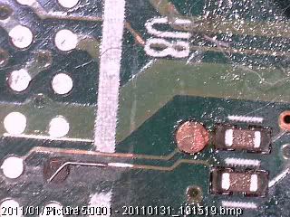
Member: 1481034 Status: Offline Sonork: Halim_Xu Thanks Meter: 3 |  Hi,Mr.Pentu i'm loosing the pad that i circled above on compaq v3000,..hw can i repair it as it has no any connectivity line as the pad u've repaired.. is it an important pad or not?thank.. |
| |
| The Following User Says Thank You to Halim_xu For This Useful Post: |
|
03-16-2011, 08:43
| #26 (permalink) | |
| Crazy Poster Join Date: Mar 2007
Posts: 59
Member: 473301 Status: Offline Thanks Meter: 11 | Quote:
| |
| |
|
03-17-2011, 08:33
| #27 (permalink) | |
| Crazy Poster Join Date: Dec 2010
Posts: 50
Member: 1481034 Status: Offline Sonork: Halim_Xu Thanks Meter: 3 | Quote:
thank a lot for your informations, my compaq v3000 using Nvidia GF-go7200 that i 've finished reball it coz the bga ic seems still good, anyway for the dummy pad i've to try to put it back on its comes out hole by glue, it should be ok right? coz yesterday i tried to fix an ATI Radeon 9600 vga for pc and it also has a dummy pad loosed, i ignored it and just soldered it back on its board after reballing it..the result it showed me nothing on monitor ( note : this vga card is working before and i take it for testing )..is that the bga ic, reballing process or the loosing pad problem???still looking for the solution..Anyway many thank for your update information mr.Pentu.. | |
| |
|
03-17-2011, 10:47
| #28 (permalink) |
| Major Poster Join Date: Apr 2010 Location: Scarborough, United Kingdon. Age: 54
Posts: 41
Member: 1285693 Status: Offline Thanks Meter: 5 | Just for your information the glue holding the pads in place softens at 150 deg C. So dont be tempted to clean the solder off the motherboard as soon as you have pulled the chip off. I know its tempting. |
| |
|
03-17-2011, 13:05
| #29 (permalink) | |
| Crazy Poster Join Date: Dec 2010
Posts: 50
Member: 1481034 Status: Offline Sonork: Halim_Xu Thanks Meter: 3 | Quote:
so the pad will sink first after the glue reach the temp 150 deg c before stick with bga ic solder balls?, any ideas besides " ignore it" as Mr. Pentu suggested for? | |
| |
|
03-17-2011, 14:03
| #30 (permalink) |
| Major Poster Join Date: Apr 2010 Location: Scarborough, United Kingdon. Age: 54
Posts: 41
Member: 1285693 Status: Offline Thanks Meter: 5 | If the pad is a dummy then its ok to leave it, but it might be an idea to also not add the ball to the chip as well, this will lower the risk of bridging if your flux bubbles. When initially cleaning the motherboard use a lot of lead solder and flux and run a ball of it over the pads using a blade tip on your soldering iron, do this without actually touching the board and let the hot solder do the work. HP boards are a pain to clean fully, this is usually the layer of tin from the intermetalic layer which has a higher melting point than 217 deg C. Also make sure all the solder has fully wetted before you pull the chip off. If you have epoxy around the chip remove as much as possible and leave the chip under the heat to make sure any balls that have been surrounded by epoxy are fully melted. Balls with epoxy around them can be a few degrees cooler than the rest that have melted. Theres a high chance you will pull the pad from either the chip or the pcb if you dont give it long enough. |
| |
| The Following User Says Thank You to Kujoy For This Useful Post: |
|
| Bookmarks |
| |
 Similar Threads
 | ||||
| Thread | Thread Starter | Forum | Replies | Last Post |
| Nokia "Contact Service" Repairer | Dirk | Nokia Legacy Phones ( DCT-1 ,2 ,3 ,L ) | 5 | 10-04-2011 05:45 |
| Repaired dead phone without backup | Prodigal | Nokia Legacy Phones ( DCT-1 ,2 ,3 ,L ) | 3 | 07-29-2011 11:26 |
| Contact Service Repairer 1.2 by Bartek | Allen | Nokia Legacy Phones ( DCT-1 ,2 ,3 ,L ) | 4 | 02-23-2011 09:00 |
| 5110 Contact Service Repairer via MBUS/FBUS | Allen | Nokia Legacy Phones ( DCT-1 ,2 ,3 ,L ) | 4 | 11-15-2010 04:17 |
| New!! Nokia Flash Checksum And Contact Service Repair | HookerGsM | Main Sales Section | 0 | 01-02-2001 10:12 |
|
|


 Linear Mode


